Nvidia is the leading manufacturer and seller of discrete graphics cards, while AMD is its arch-rival Intel will be entering the market this year. The Turing architecture released two years ago was one of the most ambitious releases by Nvidia after the reveal of CUDA, according to CEO Jensen Huang. Now the company is deciding to release the next-gen graphics cards for the data center and the enthusiast-grade gaming market. Due to concerns regarding the Coronavirus outbreak, Nvidia had to convert its premier developer conference GTC into an online-only event. It means the Corona outbreak is not holding Nvidia back from its event.
According to Wccftech, a new leak detailing specifications and performances of a mystery GPU from Nvidia has been surfaced. It could potentially be the flagship-level gaming GPUs or the data center GPUs under the rumored Ampere or Hopper architecture. The company has a history of changing names at the last hour. Speaking of nomenclature, rumors suggest that the term RTX will remain instead of the conventional GTX showing that Ray Tracing will once again be the feature of importance.
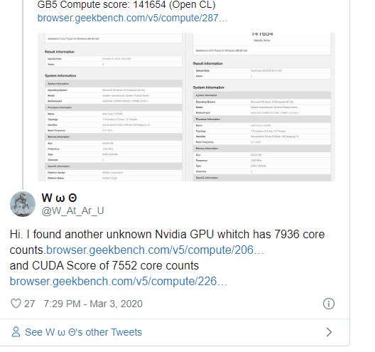
Earlier this week, a leak surfaced regarding the two GPUs, but now a new SKU has been spotted by a twitter user W_At_Ar_U. All of these chips feature a behemoth amount of CUDA cores showing that Nvidia is taking performance seriously this time. The Ampere architecture is rumored to power the upcoming Tesla GPUs, which are used to power HPC and datacenters. According to the Vice President of IT at Indiana University, Nvidia’s next-gen GPUs offer around 75% improvement in both efficiency and performance compared to the Volta GPUs released a few years ago. Some reports suggest that the performance increase is 50% with double efficiency, but we have to take these numbers with a grain of salt as these are often exaggerated.
LEAK
Since the leak is about three different GPUs serving different properties, we’ll talk about all of these separately.
GPU 1 with 7552 CUDA cores
The first GPU was leaked a few days ago by the twitter user _rogame, and it contained the specifications and Geekbench results of the mystery GPU by Nvidia. The GPU in question allegedly features 7552 CUDA cores distributed among 118 streaming multiprocessors units (SMs). To get a rough perspective about the raw computing power that the alleged graphics cards will have, TITAN RTX features 4608 CUDA cores, and Tesla V100 offers 5120 CUDA cores. The GPU core has a maximum clock speed of 1.1GHz.
Two Unknown Nvidia GPU
> 7552 Cuda cores (118 CUs)
> 1.11GHz core clock
> 24GB of memory
GB5 Compute score: 184096 (Open CL)https://t.co/rUFWACaxrg
> 6912 Cuda cores (108 CUs)
> 1.01GHz core clock
> 47GB of memory
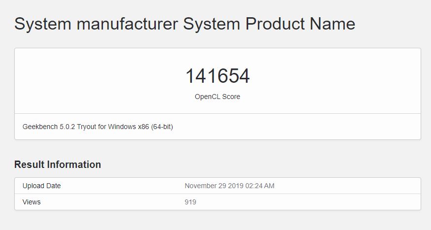
GB5 Compute score: 141654 (Open CL)https://t.co/C1jnm3sZ0D pic.twitter.com/3JrW8LrnFj
— _rogame (@_rogame) February 28, 2020
The GPU features 24GB of HBM2e memory running at 1200MHz with a 3072-bit bus. The specifications mentioned theoretically transform to 16.7TFLOP of computing power, although the clock speeds do not look final. The product, when releases, may feature a much higher boost clock speed.
Coming to the reported benchmarks, the GPU was tested on both Open CL and CUDA compute benchmarks using the Geekbench 5 benchmark software. It managed to score 184096 points, and 169368 points in the Open CL and CUDA compute benchmarks, respectively. According to the benchmark, the GPU core was only running on CUDA 8.0, which shows it requires more optimizations to run well.
GPU 2 with 6912 CUDA cores
The 2nd mystery GPU in the leak features more interesting specifications, as we will see in a bit. It contains 6912 CUDA cores clocked at 1.01GHz. The cores are spread among 108 SM, once again showing that Nvidia is sticking with 64 cores per SM regime for the generation.
The interesting bit in the leak was in the memory configuration. The GPU allegedly has 46.8GB of HBM2e memory, which seems odd. There could be two explanations for the memory size. Either Geekbench is making an error, or the GPU is specifically for the data center markets, the former seems more plausible here. The memory is clocked at 1200MHz with a bus size of 3072-bit.

Another thing to consider is the fact that the “GPU 1” had more cores but less memory. It could mean Nvidia may have GPUs specific for the workload, or we may see SKUs depending upon the memory size.
The GPU was able to score 141654 points in the CUDA compute benchmark under the Geekbench, which once again is at the lower end due to lower clock speeds.
GPU 3 with 7936 CUDA cores
Coming to the most recent leak, which shows the extent of CUDA cores on a single die. Tesla V100 had one of the biggest GPU dies since it had more than 5000 CUDA cores, and it was fabricated on TSMC’s 12nm FinFET process. The “GPU 3” in the leak has 7936 CUDA cores spread among 124 SMs. The GPU die as expected will be huge considering the 7nm standards since Ampere or Hopper architecture is rumored to be fabricated by Samsung’s EUV 7nm process.

The GPU in the leak is running at 1.1GHz clock speed, which again is not final. Moreover, it has 32GB of HBM2e memory (less than the leaked SKU of “GPU 2”) clocked at 1200MHz with the bus size of 4096-bit. All of this translates into 17.5 or 18TFLOPS of computing power. In addition to memory and core boost, the GPU packs 32MB of L2 cache, which is almost 5x more than the L2 cache supported by the Tesla V100.

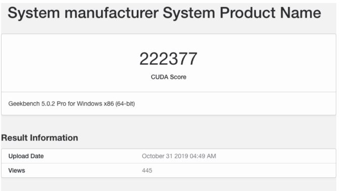
Lastly, the GPU was able to score 222377 points in the Open CL benchmark under Geekbench. It should be noted that the GPU core was running on CUDA 8.0, which shows that the GPU was not fully optimized at the time of testing. That said, the sheer specifications of the GPU are crazy enough to make one realize that it is going to be a behemoth of a GPU once it is announced. It will most probably be specialized for the HPC and datacenter market.
Finally, these are only the initial rumors of the upcoming graphics cards; the specifications may look insane right now. Still, it will become black and white once more information is released.


